 Gerardo Marx
85a774914c |
2 hours ago | |
|---|---|---|
| epwm_cpu1_bitfield | 7 days ago | |
| epwm_cpu2_driverlib | 2 weeks ago | |
| ia-presentation | 2 hours ago | |
| Readme.md | 2 hours ago | |
| pinout.jpg | 2 weeks ago | |

Readme.md
ePWM Generation, Interrupts, and Trip-Zone Protection on the TMS320F28379D
This project demonstrates how to configure the enhanced Pulse Width Modulator (ePWM) peripheral of the Texas Instruments TMS320F28379D using two register-access methods. The implementation uses CPU1 with C2000 bit-field structures and CPU2 with HWREG() / HWREGH() register access from driverlib.
The guide follows an incremental approach: begin with an almost-empty program, find the relevant peripheral registers in C2000Ware, configure one submodule at a time, and verify each result with an oscilloscope. The supplied source files serve as the initial examples; any identified concerns are documented at the end rather than being changed without notice.
1. Hardware and software requirements
- TMS320F28379D microcontroller or compatible board (confirm that the listed GPIOs are exposed); we are using the
LAUNCHXL-F28379Dboard development kit. - Code Composer Studio (CCS), version 20.5.0 or above.
- C2000Ware and its device-support headers and/or driverlib, or previously installed the
C2000Ware_26_00_00_00. - Oscilloscope or logic analyzer to observe PWM and diagnostic GPIOs.
- A safe logic-level input or suitable test switch for trip-zone experiments.
- Initially do not connect the PWM signals to power semiconductor gates; verify the outputs and fault response at logic level.
Timing assumption: the examples configure an ePWM module input clock of 100 MHz and the time-base clock (TBCLK) of 50 MHz. The device system clock, EPWMCLKDIV, HSPCLKDIV, and CLKDIV must agree with these assumptions.
2. Project objectives and expected behavior
The two source files are pwm_cpu1_bitfield.c and pwm_cpu2_driverlib.c.
| CPU | ePWM | Outputs | Counter mode | Intended PWM frequency | Initial comparison |
|---|---|---|---|---|---|
| CPU1 | ePWM1 | GPIO0 / GPIO1 | Up-count (sawtooth counter) | 10 kHz | CMPA = 1999, approximately 40% |
| CPU1 | ePWM2 | GPIO2 / GPIO3 | Up-down (triangular counter) | 5 kHz | CMPA = 1750, parameter m = -0.3 |
| CPU2 | ePWM4 | GPIO6 / GPIO7 | Up-count (sawtooth counter) | approximately 15 kHz | CMPA = 1999, approximately 60% |
| CPU2 | ePWM5 | GPIO8 / GPIO9 | Up-down (triangular counter) | 4 kHz | code uses m = +0.7, subject to review |
Additional tasks:
- ePWM1 interrupt: intended at
TBCTR = 0, once per PWM cycle; toggle GPIO22. - ePWM5 interrupt: intended at
TBCTR = 0andTBCTR = TBPRD, twice per PWM cycle; toggle GPIO52. - Trip-zone input: GPIO97 is routed through Input X-BAR 1 as
TZ1to request a one-shot shutdown of ePWM1, ePWM2, ePWM4, and ePWM5 outputs. - Trip-zone ISRs: CPU1 receives ePWM1/ePWM2 trip interrupts; CPU2 receives ePWM4/ePWM5 trip interrupts.
The output pairs use the dead-band submodule. The two signals must be checked on the oscilloscope: do not assume complementary outputs are safe for a power stage without measuring the dead time and fault behavior.
3. General program flow
CPU1
- Initialize system clocks and the interrupt controller.
- Select ePWM clock division and assign peripheral ownership across CPU1/CPU2.
- Enable the clock gates for ePWM1/ePWM2.
- Disable
TBCLKSYNCwhile preparing the time-base counters. - Configure time-base (
TB), counter-compare (CC), action qualifier (AQ), and dead-band (DB). - Configure event trigger (
ET) for ePWM1 and trip zone (TZ) for ePWM1/ePWM2. - Register the ePWM and trip-zone interrupt service routines.
- Configure GPIO0–GPIO3, diagnostic GPIO22, the GPIO52 ownership, and Input X-BAR from GPIO97.
- Clear initial interrupt/fault flags as appropriate only after confirming the fault is inactive.
- Enable synchronization after both CPUs are ready, then enter the main loop.
CPU2
- Initialize the interrupt controller and vector table.
- Enable the clock gates for ePWM4/ePWM5 on CPU2.
- Configure
TB,CC,AQ, andDBwith direct register operations. - Configure the ePWM5 event-trigger interrupt and the ePWM4/ePWM5 trip zones.
- Register and enable the CPU2 interrupt paths.
- Signal configuration readiness to CPU1 using an explicit interprocessor synchronization mechanism.
- Enter the main loop.
Dual-core note: CPU1 controls cross-CPU ownership selection and shared startup coordination. Independent writes to TBCLKSYNC from both programs do not constitute a reliable synchronization protocol.
4.0 Create a dual CPU project ready for bitfield and driverlib
- Open a new folder (5-epwm-example); not a workspace
- Import project from
C2000Ware_26_01_00_00:driverlib/f2837xd/examples/dual/empty_projects/css - Change folder/project names
pwm_cpu1_bitfield.pwm_cpu2_driverlib
- Change the
.cfiles also; follow the same approach - Bitfield project needs some additional compilation variables
- Path type var named
C2000_Commonpoints to/Users/gmarx/ti/C2000Ware_26_01_00_00/device_support/f2837xd/common/include - Path type var named
C2000_Headerspointing to/Users/gmarx/ti/C2000Ware_26_01_00_00/device_support/f2837xd/headers/include
- Path type var named
- Also, in
C2000 CompilerandInclude Options, we should add the previously created vars as:${C2000_Common}${C2000_Headers}
- Additionally, at
C2000 CompilerandPredefined Symbols, add the entry:_DUAL_HEADERSand_LAUNCHXL_F28379D.
- Additional source files must be added from
/Users/gmarx/ti/C2000Ware_26_00_00_00/device_support/f2837xd/common/source:F2837xD_SysCtrl.cF2837xD_usDelay.asmF2837xD_EPwm.c
- Add the file
F2837xD_GlobalVariableDefs.c-data structure to map all peripherals- that is at/Users/gmarx/ti/C2000Ware_26_00_00_00/device_support/f2837xd/headers/source/F2837xD_GlobalVariableDefs.c - One last file must be included:
F2837xD_Headers_nonBIOS_cpu1.cmdfrom the path/Users/gmarx/ti/C2000Ware_26_00_00_00/device_support/f2837xd/headers/cmd/F2837xD_Headers_nonBIOS_cpu1.cmdwe are using the nonBIOS option because the code will run in debug mode - However, the CPU2 has an issue at the
Predefined symbols, we must change the nameCPU1toCPU2
- From the 12 PWMs, only 6 are available
- PWM1 (PWM1A and PWM1B) and PWM2 will be used for CPU1
- PWM4 and PWM5 will be used for CPU2
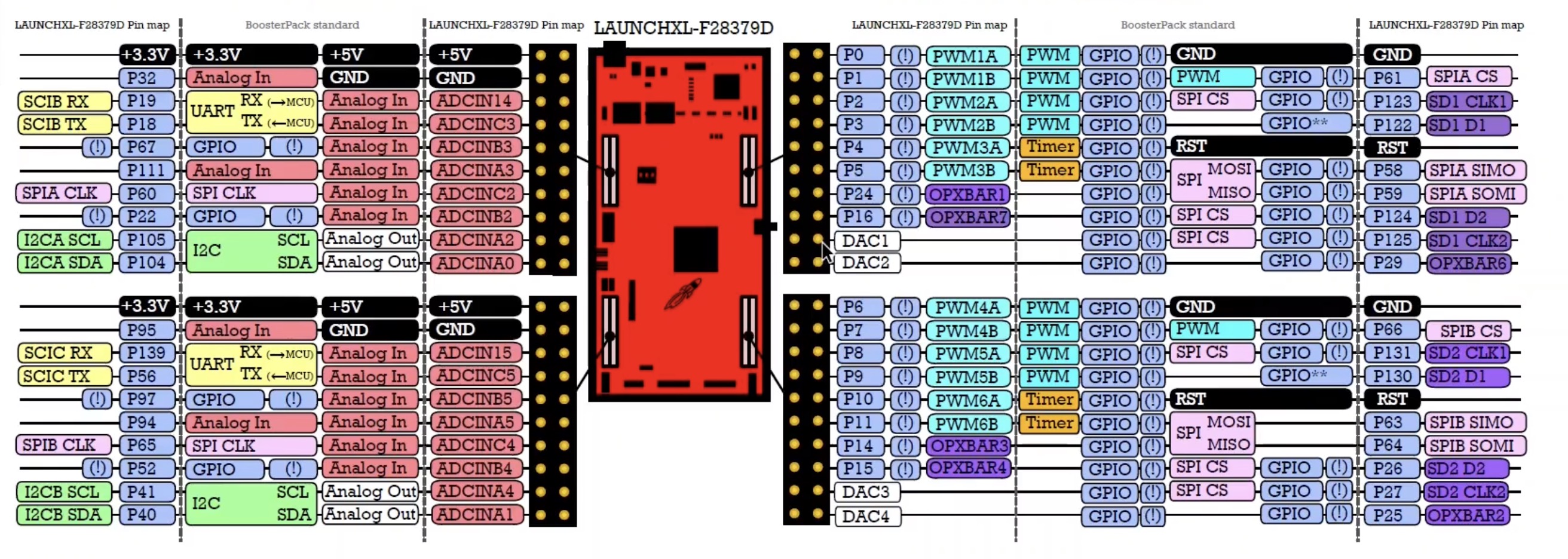
4. Start from an almost-empty CPU1 program (bit-field approach)
#include "F28x_Project.h"
#include "driverlib.h"
#include "device.h"

__interrupt void epwm1_isr(void) { /* TODO */ }
__interrupt void epwm1_trip_isr(void) { /* TODO */ }
__interrupt void epwm2_trip_isr(void) { /* TODO */ }

void main(void)
{
    // 1. Initialize the system and interrupts.
    // 2. Select ePWM clocks and assign CPU ownership.
    // 3. Enable ePWM1 and ePWM2 clocks.
    // 4. Stop time-base synchronization.
    // 5. Configure TB and CC.
    // 6. Configure AQ and dead band.
    // 7. Configure event triggers and trip zones.
    // 8. Register and enable interrupts.
    // 9. Configure PWM GPIOs, diagnostic pins, and X-BAR.
    // 10. Confirm fault conditions and synchronize startup.
    for (;;) {}
}
The following sections progressively fill in these steps. Register names are those used in the provided source.
Note: we are in video ePWM part 2
5 CPU1 code
initial steps
CLK_CFG_REGSRegisters (section 3.17.11)-> PERCLKDIVSEL -> F2837xD_sysctrl.hDEV_CFG_REGS(section 3.17.10), same fileCPU_SYS_REGS(section 3.17.12) -> PCLKCR2 register has the pwm bits -> F2837xD_sysctrl.h -> search for the structCPU_SYS_REGSTBCLKSYNCbitEPWM_REGSRegisters (section 15.15.2)
#include "F28x_Project.h"
#include "driverlib.h"
#include "device.h"

__interrupt void epwm1_isr(void) { /* TODO */ }
__interrupt void epwm1_trip_isr(void) { /* TODO */ }
__interrupt void epwm2_trip_isr(void) { /* TODO */ }

void main(void)
{
    // 1. Initialize the system and interrupts.
    InitSysCtrl();
    EALLOW;
    ClkCfgRegs.PERCLKDIVSEL.bit.EPWMCLKDIV = 1;
    EDIS;

    // 2. Select ePWM clocks and assign CPU ownership.
    EALLOW;
    DevCfgRegs.CPUSEL0.bit.EPWM1 = 0; //cpu0
    DevCfgRegs.CPUSEL0.bit.EPWM2 = 0;
    DevCfgRegs.CPUSEL0.bit.EPWM4 = 1; //cpu1
    DevCfgRegs.CPUSEL0.bit.EPWM5 = 1;
    EDIS;

    // 3. Enable ePWM1 and ePWM2 clocks.
    EALLOW;
    CpuSysRegs.PCLKCR2.bit.EPWM1 = 1;
    CpuSysRegs.PCLKCR2.bit.EPWM2 = 1;
    EDIS;

    // 4. Stop time-base synchronization.
    EALLOW;
    CpuSysRegs.PCLKCR0.bit.TBCLKSYNC = 1; //stop the timer
    EDIS;

    // 5. Configure TB and CC.
    // Configure the eWM modules 1 and 2
		// Time base sub-module
		// 100 MHz. TBCLK = 100 / (2 * 1) = 50 Mhz
		EPwm1Regs.TBCTL.bit.FREE_SOFT = 2; // 2 or 3
		EPwm1Regs.TBCTL.bit.CLKDIV = 0; I
		EPwm1Regs.TBCTL.bit.HSPCLKDIV = 1;
		EPwm1Regs.TBCTL.bit.PRDLD = 0;
		EPwm1Regs.TBCTL.bit.CTRMODE = 0;

		EPwm2Regs.TBCTL.bit.FREE_SOFT = 2; // 2 or 3
		EPwm2Regs.TBCTL.bit.CLKDIV = 0; I
		EPwm2Regs.TBCTL.bit.HSPCLKDIV = 1;
		EPwm2Regs.TBCTL.bit.PRDLD = 0;
		EPwm2Regs.TBCTL.bit.CTRMODE = 2; // up-down count mode

		//Period registers
		EPwm1Regs. TBPRD = 5000 - 1; // 10 kHz sawtooth
		EPwm2Regs. TBPRD = 5000;      // 5 kHz triangular

		// Counter-compare sub-module
		EPwm1Regs.CMPCTL.bit.SHDWAMODE = 0;
		EPwm1Regs.CMPCTL.bit.LOADAMODE = 0;

		EPwm1Regs.CMPA.bit.CMPA = 1999;

		EPwm2Regs.CMPCTL.bit.SHDWAMODE = 0;
		EPwm2Regs.CMPCTL.bit.LOADAMODE = 0;

		EPwm2Regs. CMPA.bit. CMPA = (uint16_t) ( ((-0.3+1)/2.0) * 5000 );

    // 6. Configure AQ and dead band.

    // Action qualifier sub-module
		// ePWM1 - A output to be fed to the upper device of a leg
		// B output to be fed to the lower device of a leg
		// TBCTR = 0, A will be high, B will be low (ZRO - AQCTLA/B)
		// TBCTR = CMPA. A will be low and B will be high (CAU - AQCTLA/B)
		EPwm1Regs. AQCTLA.bit.ZRO = 2;
		EPwm1Regs .AQCTLB.bit.ZRO = 1;
		EPwm1Regs .AQCTLA.bit.CAU = 1;
		EPwm1Regs.AQCTLB.bit.CAU = 2;

		// ePWM2 - A output to be fed to the upper device of a leg
		// B output to be fed to the lower device of a leg
		// TBCTR = CMPA first half, A will be high, B will be low (CAU - AQCTLA/B)
		// TBCTR = CMPA second half. A will be low and B will be high (CAD - AQCTLA/B)

		EPwm2Regs. AQCTLA.bit.ZROI = 2;
		EPwm2Regs .AQCTLB.bit.ZRO = 1;
		EPwm2Regs. AQCTLA.bit.CAU = 1;
		EPwm2Regs. AQCTLB.bit.CAU = 2;
    // 7. Configure event triggers and trip zones.
    // 8. Register and enable interrupts.
    // 9. Configure PWM GPIOs, diagnostic pins, and X-BAR.
    // 10. Confirm fault conditions and synchronize startup.
    for (;;) {}
}
Configuring actions
#include "F28x_Project.h"
#include "driverlib.h"
#include "device.h"

__interrupt void epwm1_isr(void) { /* TODO */ }
__interrupt void epwm1_trip_isr(void) { /* TODO */ }
__interrupt void epwm2_trip_isr(void) { /* TODO */ }

void main(void)
{
    // 1. Initialize the system and interrupts.
    InitSysCtrl();
    EALLOW;
    ClkCfgRegs.PERCLKDIVSEL.bit.EPWMCLKDIV = 1;
    EDIS;

    // 2. Select ePWM clocks and assign CPU ownership.
    EALLOW;
    DevCfgRegs.CPUSEL0.bit.EPWM1 = 0; //cpu0
    DevCfgRegs.CPUSEL0.bit.EPWM2 = 0;
    DevCfgRegs.CPUSEL0.bit.EPWM4 = 1; //cpu1
    DevCfgRegs.CPUSEL0.bit.EPWM5 = 1;
    EDIS;

    // 3. Enable ePWM1 and ePWM2 clocks.
    EALLOW;
    CpuSysRegs.PCLKCR2.bit.EPWM1 = 1;
    CpuSysRegs.PCLKCR2.bit.EPWM2 = 1;
    EDIS;

    // 4. Stop time-base synchronization.
    EALLOW;
    CpuSysRegs.PCLKCR0.bit.TBCLKSYNC = 1; //stop the timer
    EDIS;

    // 5. Configure TB and CC.
    // Configure the eWM modules 1 and 2
		// Time base sub-module
		// 100 MHz. TBCLK = 100 / (2 * 1) = 50 Mhz
		EPwm1Regs.TBCTL.bit.FREE_SOFT = 2; // 2 or 3
		EPwm1Regs.TBCTL.bit.CLKDIV = 0; I
		EPwm1Regs.TBCTL.bit.HSPCLKDIV = 1;
		EPwm1Regs.TBCTL.bit.PRDLD = 0;
		EPwm1Regs.TBCTL.bit.CTRMODE = 0;

		EPwm2Regs.TBCTL.bit.FREE_SOFT = 2; // 2 or 3
		EPwm2Regs.TBCTL.bit.CLKDIV = 0; I
		EPwm2Regs.TBCTL.bit.HSPCLKDIV = 1;
		EPwm2Regs.TBCTL.bit.PRDLD = 0;
		EPwm2Regs.TBCTL.bit.CTRMODE = 2; // up-down count mode

		//Period registers
		EPwm1Regs. TBPRD = 5000 - 1; // 10 kHz sawtooth
		EPwm2Regs. TBPRD = 5000;      // 5 kHz triangular

		// Counter-compare sub-module
		EPwm1Regs.CMPCTL.bit.SHDWAMODE = 0;
		EPwm1Regs.CMPCTL.bit.LOADAMODE = 0;

		EPwm1Regs.CMPA.bit.CMPA = 1999;

		EPwm2Regs.CMPCTL.bit.SHDWAMODE = 0;
		EPwm2Regs.CMPCTL.bit.LOADAMODE = 0;

		EPwm2Regs. CMPA.bit. CMPA = (uint16_t) ( ((-0.3+1)/2.0) * 5000 );

    // 6. Configure AQ and dead band.

    // Action qualifier sub-module
		// ePWM1 - A output to be fed to the upper device of a leg
		// B output to be fed to the lower device of a leg
		// TBCTR = 0, A will be high, B will be low (ZRO - AQCTLA/B)
		// TBCTR = CMPA. A will be low and B will be high (CAU - AQCTLA/B)
		EPwm1Regs. AQCTLA.bit.ZRO = 2;
		EPwm1Regs .AQCTLB.bit.ZRO = 1;
		EPwm1Regs .AQCTLA.bit.CAU = 1;
		EPwm1Regs.AQCTLB.bit.CAU = 2;

		// ePWM2 - A output to be fed to the upper device of a leg
		// B output to be fed to the lower device of a leg
		// TBCTR = CMPA first half, A will be high, B will be low (CAU - AQCTLA/B)
		// TBCTR = CMPA second half. A will be low and B will be high (CAD - AQCTLA/B)

		EPwm2Regs. AQCTLA.bit.ZROI = 2;
		EPwm2Regs .AQCTLB.bit.ZRO = 1;
		EPwm2Regs. AQCTLA.bit.CAU = 1;
		EPwm2Regs. AQCTLB.bit.CAU = 2;
    // 7. Configure event triggers and trip zones.
    // 8. Register and enable interrupts.
    // 9. Configure PWM GPIOs, diagnostic pins, and X-BAR.
    // 10. Confirm fault conditions and synchronize startup.
    for (;;) {}
}
5. CPU1: system initialization and peripheral ownership
The provided source initializes the system and interrupt tables:
InitSysCtrl(); // <---
InitPieCtrl();
IER = 0x0000;
IFR = 0x0000;
InitPieVectTable();
The CPU1 program sets the ePWM module input clock divisor and allocates the peripherals —CLK_CFG_REGS Registers -> PERCLKDIVSEL -> F2837xD_sysctrl.h—:
EALLOW;
ClkCfgRegs.PERCLKDIVSEL.bit.EPWMCLKDIV = 1; // <---
DevCfgRegs.CPUSEL0.bit.EPWM1 = 0;
DevCfgRegs.CPUSEL0.bit.EPWM2 = 0;
DevCfgRegs.CPUSEL0.bit.EPWM4 = 1;
DevCfgRegs.CPUSEL0.bit.EPWM5 = 1;
EDIS;
0indicates CPU1 ownership and1indicates CPU2 ownership in these fields.- Establish peripheral ownership before CPU2 configures its modules.
- Check the resulting
EPWMCLKfrom the actual system clock and clock-divider settings.
Enable the CPU1 modules and stop time-base synchronization during setup:
EALLOW;
CpuSysRegs.PCLKCR2.bit.EPWM1 = 1;
CpuSysRegs.PCLKCR2.bit.EPWM2 = 1;
CpuSysRegs.PCLKCR0.bit.TBCLKSYNC = 0;
EDIS;
Register research: locate the definitions of CPUSEL0, PCLKCR2, PCLKCR0, and PERCLKDIVSEL in the F2837xD device headers. Record their bit fields and the clock/ownership dependencies.
6. CPU1: time-base submodule (TB)
The time-base submodule selects counter mode and defines the switching period.
// ePWM1: up-count
EPwm1Regs.TBCTL.bit.FREE_SOFT = 2;
EPwm1Regs.TBCTL.bit.CLKDIV = 0;
EPwm1Regs.TBCTL.bit.HSPCLKDIV = 1;
EPwm1Regs.TBCTL.bit.PRDLD = 0;
EPwm1Regs.TBCTL.bit.CTRMODE = 0;
EPwm1Regs.TBPRD = 5000 - 1;

// ePWM2: up-down count
EPwm2Regs.TBCTL.bit.FREE_SOFT = 2;
EPwm2Regs.TBCTL.bit.CLKDIV = 0;
EPwm2Regs.TBCTL.bit.HSPCLKDIV = 1;
EPwm2Regs.TBCTL.bit.PRDLD = 0;
EPwm2Regs.TBCTL.bit.CTRMODE = 2;
EPwm2Regs.TBPRD = 5000;
With the assumed clock:
f_{TBCLK}=\frac{100\ \mathrm{MHz}}{2\cdot1}=50\ \mathrm{MHz}.
For up-count mode, using a zero-based period register:
f_{PWM}\approx\frac{f_{TBCLK}}{TBPRD+1}.
For up-down mode:
f_{PWM}=\frac{f_{TBCLK}}{2TBPRD}.
Therefore:
- ePWM1:
TBPRD = 4999→ 10 kHz. - ePWM2:
TBPRD = 5000→ 5 kHz.
Exercise: use the oscilloscope to compare the PWM periods of the up-count and up-down examples. Explain why an up-down counter requires twice as many TBCLK ticks for a complete PWM period.
7. CPU1: counter-compare submodule (CC)
The compare register determines the positions of edges generated by the action qualifier.
// ePWM1
EPwm1Regs.CMPCTL.bit.SHDWAMODE = 0;
EPwm1Regs.CMPCTL.bit.LOADAMODE = 0;
EPwm1Regs.CMPA.bit.CMPA = 1999;

// ePWM2
EPwm2Regs.CMPCTL.bit.SHDWAMODE = 0;
EPwm2Regs.CMPCTL.bit.LOADAMODE = 0;
EPwm2Regs.CMPA.bit.CMPA =
    (uint16_t)(((-0.3 + 1.0) / 2.0) * 5000);
For the pre-dead-band ePWM1 A waveform with high at zero and low at CAU, a useful nominal approximation is:
D\approx\frac{CMPA}{TBPRD+1}=\frac{1999}{5000}\approx 0.40.
The ePWM2 source defines an initial modulation parameter, not a continuously varying modulation signal:
CMPA=\frac{m+1}{2}TBPRD,
\qquad m=-0.3\Rightarrow CMPA=1750.
The requested modulation range -0.97 to +0.97 appears in the source-file comments, but the supplied example does not implement a time-varying modulation algorithm. Students can later update CMPA periodically to implement one.
Exercise: derive CMPA for m = 0, m = +0.5, and m = -0.5. Explain the waveform using the action-qualifier edge definitions; do not assume the modulation parameter is numerically equal to the final PWM duty cycle.
8. CPU1: action-qualifier submodule (AQ)
The action qualifier converts timer events into logic-level transitions.
| Event | Description | Relevant fields |
|---|---|---|
ZRO |
Counter reaches zero | AQCTLA.ZRO, AQCTLB.ZRO |
CAU |
Up-count reaches compare A | AQCTLA.CAU, AQCTLB.CAU |
CAD |
Down-count reaches compare A | AQCTLA.CAD, AQCTLB.CAD |
// ePWM1: initial high at zero, low at up-count CMPA
EPwm1Regs.AQCTLA.bit.ZRO = 2;
EPwm1Regs.AQCTLB.bit.ZRO = 2;
EPwm1Regs.AQCTLA.bit.CAU = 1;
EPwm1Regs.AQCTLB.bit.CAU = 1;

// ePWM2: high on up CMPA, low on down CMPA
EPwm2Regs.AQCTLA.bit.CAU = 2;
EPwm2Regs.AQCTLB.bit.CAU = 2;
EPwm2Regs.AQCTLA.bit.CAD = 1;
EPwm2Regs.AQCTLB.bit.CAD = 1;
The source configures both pre-dead-band A and B paths with matching actions; the desired output polarity is subsequently generated using the dead-band polarity selection. Distinguish between signals before dead band and physical ePWMxA/ePWMxB pins.
9. CPU1: dead-band submodule (DB)
Dead band introduces timing separation between switching transitions. The supplied code selects two delay generators and a polarity arrangement:
EPwm1Regs.DBCTL.bit.IN_MODE = 1;
EPwm1Regs.DBCTL.bit.POLSEL = 2;
EPwm1Regs.DBCTL.bit.OUT_MODE = 3;
EPwm1Regs.DBRED.all = 100;
EPwm1Regs.DBFED.all = 100;

EPwm2Regs.DBCTL.bit.IN_MODE = 1;
EPwm2Regs.DBCTL.bit.POLSEL = 2;
EPwm2Regs.DBCTL.bit.OUT_MODE = 3;
EPwm2Regs.DBRED.all = 250;
EPwm2Regs.DBFED.all = 250;
For TBCLK = 50 MHz, assuming the dead-band counter uses the same clock and no additional division:
t_{DB}=\frac{DBRED\text{ or }DBFED}{50\times10^6}.
| Module | DBRED | DBFED | Nominal rising/falling delay |
|---|---|---|---|
| ePWM1 | 100 | 100 | 2 µs |
| ePWM2 | 250 | 250 | 5 µs |
Exercise: measure the time between relevant complementary output transitions. Confirm that no overlapping high pulses occur; also calculate whether the desired minimum pulse width can accommodate the chosen dead time.
10. CPU1: ePWM1 event-trigger interrupt
The supplied code generates an interrupt when the counter reaches zero, nominally once each 10 kHz PWM period:
EPwm1Regs.ETSEL.bit.INTEN = 1;
EPwm1Regs.ETSEL.bit.INTSEL = 1;
EPwm1Regs.ETPS.bit.INTPRD = 1;
Register the handler and enable its PIE/CPU paths:
EALLOW;
PieVectTable.EPWM1_INT = &epwm1_isr;
EDIS;
PieCtrlRegs.PIEIER3.bit.INTx1 = 1;
IER |= 0x4U;  // CPU interrupt group 3
The ISR from the source toggles GPIO22, clears the ePWM flag, and acknowledges PIE group 3:
__interrupt void epwm1_isr(void)
{
    GpioDataRegs.GPATOGGLE.bit.GPIO22 = 1;
    EPwm1Regs.ETCLR.bit.INT = 1;
    PieCtrlRegs.PIEACK.bit.ACK3 = 1;
}
Since each ISR toggles rather than emits a complete pulse, GPIO22 should have an idealized waveform frequency of 5 kHz, even though the interrupt rate is 10 kHz. This assumes the CPU can reliably service all interrupts.
Exercise: measure GPIO22 independently from GPIO0 and identify the difference between PWM frequency, interrupt frequency, and toggle-output frequency.
11. CPU1: one-shot trip-zone protection
The supplied project routes GPIO97 through INPUT1SELECT and enables the TZ1 one-shot source in both ePWM modules:
EALLOW;
InputXbarRegs.INPUT1SELECT = 97U;

EPwm1Regs.TZSEL.bit.OSHT1 = 1;
EPwm1Regs.TZCTL.bit.TZA = 2;
EPwm1Regs.TZCTL.bit.TZB = 2;
EPwm1Regs.TZEINT.bit.OST = 1;

EPwm2Regs.TZSEL.bit.OSHT1 = 1;
EPwm2Regs.TZCTL.bit.TZA = 2;
EPwm2Regs.TZCTL.bit.TZB = 2;
EPwm2Regs.TZEINT.bit.OST = 1;
EDIS;
The TZA = 2 and TZB = 2 actions select force-low behavior for the corresponding ePWM outputs. The one-shot fault is designed to latch until software explicitly clears it.
Enable both trip-zone interrupts:
EALLOW;
PieVectTable.EPWM1_TZ_INT = &epwm1_trip_isr;
PieVectTable.EPWM2_TZ_INT = &epwm2_trip_isr;
EDIS;
PieCtrlRegs.PIEIER2.bit.INTx1 = 1;
PieCtrlRegs.PIEIER2.bit.INTx2 = 1;
IER |= 0x2U;  // CPU interrupt group 2
Important protection rule: the original CPU1 ISRs clear TZCLR.INT and TZCLR.OST immediately. This is not an adequate fault-latching strategy for an actual power converter. For a safe experiment, record the fault and keep PWM inhibited until the input is no longer active and a deliberate software restart has been performed. Do not automatically clear the one-shot latch within the trip ISR merely to resume operation.
Also confirm GPIO97's input pad, multiplexing, and qualification are correctly configured on the selected board, and test the active polarity. Setting INPUT1SELECT alone does not fully document the external electrical behavior of that pin.
12. CPU1: GPIO setup and startup
The original program sets GPIO0–GPIO3 for ePWM1A/B and ePWM2A/B, GPIO22 for interrupt diagnostics, and GPIO52 for CPU2 diagnostics. For example:
EALLOW;
GpioCtrlRegs.GPAGMUX1.bit.GPIO0 = 0;
GpioCtrlRegs.GPAMUX1.bit.GPIO0 = 1;
GpioCtrlRegs.GPAGMUX1.bit.GPIO1 = 0;
GpioCtrlRegs.GPAMUX1.bit.GPIO1 = 1;
GpioCtrlRegs.GPAGMUX1.bit.GPIO2 = 0;
GpioCtrlRegs.GPAMUX1.bit.GPIO2 = 1;
GpioCtrlRegs.GPAGMUX1.bit.GPIO3 = 0;
GpioCtrlRegs.GPAMUX1.bit.GPIO3 = 1;

GpioCtrlRegs.GPAGMUX2.bit.GPIO22 = 0;
GpioCtrlRegs.GPAMUX2.bit.GPIO22 = 0;
GpioCtrlRegs.GPADIR.bit.GPIO22 = 1;

GpioCtrlRegs.GPBGMUX2.bit.GPIO52 = 0;
GpioCtrlRegs.GPBMUX2.bit.GPIO52 = 0;
GpioCtrlRegs.GPBDIR.bit.GPIO52 = 1;
GpioCtrlRegs.GPBCSEL3.bit.GPIO52 = 2; // CPU2 ownership
EDIS;
The supplied source also configures GPIO6–GPIO9 on CPU1 for ePWM4/ePWM5 output routing. Keep this separate from the CPU2 ePWM module configuration; CPU ownership of an ePWM peripheral is not identical to ownership of an individual GPIO pin.
Before enabling TBCLKSYNC, ensure CPU2 configuration is complete, protective inputs are in an appropriate state, and initial flags are handled. The source currently ends with:
EALLOW;
CpuSysRegs.PCLKCR0.bit.TBCLKSYNC = 1;
EDIS;
for (;;) {}
A complete dual-core laboratory example should introduce a startup handshake so this action occurs only after both cores finish configuration.
13. CPU2: start from an almost-empty program (HWREG approach)
#include "driverlib.h"
#include "device.h"

__interrupt void epwm5_isr(void) { /* TODO */ }
__interrupt void epwm4_trip_isr(void) { /* TODO */ }
__interrupt void epwm5_trip_isr(void) { /* TODO */ }

void main(void)
{
    // 1. Initialize CPU2 interrupt module and vector table.
    // 2. Enable ePWM4 and ePWM5 peripheral clocks.
    // 3. Configure time-base and counter-compare registers.
    // 4. Configure action qualifiers and dead band.
    // 5. Configure event triggers and trip zones.
    // 6. Register and enable interrupts.
    // 7. Notify CPU1 that CPU2 configuration is complete.
    for (;;) {}
}
For this section, the student should locate:
hw_memmap.h: peripheral base addresses such asEPWM4_BASE,EPWM5_BASE,CPUSYS_BASE.hw_epwm.h: offsets such asEPWM_O_TBCTL,EPWM_O_CMPA,EPWM_O_AQCTLA, andEPWM_O_TZCLR.hw_sysctl.h: clock-gate register offsets.hw_pie.handhw_ints.h: PIE register offsets and interrupt-vector identifiers.
HWREGH(address) accesses a 16-bit register location, while HWREG(address) accesses a 32-bit register location. For CMPA, students should determine whether a 32-bit access covers both CMPA and CMPAHR; never assume an arbitrary bit mask or |= operation overwrites all intended compare bits.
14. CPU2: initialize modules and configure the time base
Interrupt_initModule();
Interrupt_initVectorTable();

EALLOW;
HWREG(CPUSYS_BASE + SYSCTL_O_PCLKCR2) |= (uint32_t)0x18U;
EDIS;

// Time-base: values from the supplied CPU2 program
HWREGH(EPWM4_BASE + EPWM_O_TBCTL) = 0xC080;
HWREGH(EPWM5_BASE + EPWM_O_TBCTL) = 0xC082;
HWREGH(EPWM4_BASE + EPWM_O_TBPRD) = 3333 - 1;
HWREGH(EPWM5_BASE + EPWM_O_TBPRD) = 6250;
The TBCTL register words encode free-run debug behavior, clock prescalers, and up/up-down counter selection. Students should decode every bit field using the TI technical reference manual before using these values.
With TBCLK = 50 MHz:
- ePWM4:
50 MHz / 3333 ≈ 15.0015 kHz. - ePWM5:
50 MHz / (2 × 6250) = 4 kHz.
The CPU2 source also clears the TBCLKSYNC bit during configuration and sets it again at the end. In the final dual-core application, replace this unsynchronized startup behavior with a CPU1-coordinated release.
15. CPU2: counter comparison and action qualifier
The supplied code uses:
// Configure CMPCTL shadow/load bits.
HWREGH(EPWM4_BASE + EPWM_O_CMPCTL) &= 0xffefU;
HWREGH(EPWM4_BASE + EPWM_O_CMPCTL) &= 0xfffcU;
HWREGH(EPWM4_BASE + EPWM_O_CMPA) |= (uint32_t)0x07CF0000U;

HWREGH(EPWM5_BASE + EPWM_O_CMPCTL) &= 0xffefU;
HWREGH(EPWM5_BASE + EPWM_O_CMPCTL) &= 0xfffcU;
HWREGH(EPWM5_BASE + EPWM_O_CMPA + 1) =
    (uint16_t)(((0.7 + 1.0) / 2.0) * 5000);
The ePWM4 compare constant encodes 0x07CF = 1999 as the upper 16-bit comparison value. Review the |= access before using it repeatedly because it does not clear previous compare bits. The CPU2 ePWM5 line computes 4250 from a hard-coded 5000, whereas its actual TBPRD is 6250. If the intended formula is (m + 1) × TBPRD / 2, the result for m = 0.7 should be 5312 after C conversion to an integer (the unrounded mathematical result is 5312.5). This is a source-code discrepancy to correct as a student exercise.
The source configures the AQ registers with these writes:
// ePWM4: high at ZRO, low at CAU
HWREGH(EPWM4_BASE + EPWM_O_AQCTLA) = 0;
HWREGH(EPWM4_BASE + EPWM_O_AQCTLB) = 0;
HWREGH(EPWM4_BASE + EPWM_O_AQCTLA) |= 0x0002U;
HWREGH(EPWM4_BASE + EPWM_O_AQCTLB) |= 0x0002U;
HWREGH(EPWM4_BASE + EPWM_O_AQCTLA) |= 0x0010U;
HWREGH(EPWM4_BASE + EPWM_O_AQCTLB) |= 0x0010U;

// ePWM5: high at CAU, low at CAD
HWREGH(EPWM5_BASE + EPWM_O_AQCTLA) = 0;
HWREGH(EPWM5_BASE + EPWM_O_AQCTLB) = 0;
HWREGH(EPWM5_BASE + EPWM_O_AQCTLA) |= 0x0020U;
HWREGH(EPWM5_BASE + EPWM_O_AQCTLB) |= 0x0020U;
HWREGH(EPWM5_BASE + EPWM_O_AQCTLA) |= 0x0040U;
HWREGH(EPWM5_BASE + EPWM_O_AQCTLB) |= 0x0040U;
Exercise: identify which bits correspond to the ZRO, CAU, and CAD fields, and reproduce the expected output-edge sequence before inserting dead band.
16. CPU2: dead-band setup
HWREGH(EPWM4_BASE + EPWM_O_DBCTL) = (uint16_t)0x1BU;
HWREGH(EPWM4_BASE + EPWM_O_DBRED) = 100;
HWREGH(EPWM4_BASE + EPWM_O_DBFED) = 100;

HWREGH(EPWM5_BASE + EPWM_O_DBCTL) = (uint16_t)0x1BU;
HWREGH(EPWM5_BASE + EPWM_O_DBRED) = 250;
HWREGH(EPWM5_BASE + EPWM_O_DBFED) = 250;
These are the CPU2 register-word equivalents of the CPU1 dead-band setup. The intended delays are 2 µs for ePWM4 and 5 µs for ePWM5 under the assumed 50 MHz clock.
17. CPU2: ePWM5 interrupt and GPIO52 diagnostic
The provided CPU2 program writes:
HWREGH(EPWM5_BASE + EPWM_O_ETSEL) |= (uint16_t)0xBU;
HWREGH(EPWM5_BASE + EPWM_O_ETPS) |= (uint16_t)0x1U;
ETSEL = 0x000B enables interrupt generation with selection INTSEL = 3 (counter zero OR counter period). In up-down mode, this creates two selected events in one PWM cycle. ETPS.INTPRD = 1 selects every event.
__interrupt void epwm5_isr(void)
{
    HWREG(GPIODATA_BASE + GPIO_O_GPBTOGGLE) = (uint32_t)0x100000U;
    HWREGH(EPWM5_BASE + EPWM_O_ETCLR) |= (uint16_t)0x1U;
    HWREGH(PIECTRL_BASE + PIE_O_ACK) |= (uint16_t)0x4U;
}
If all interrupts are serviced, two events per 4 kHz PWM cycle imply an 8 kHz interrupt rate and a 4 kHz GPIO52 toggle waveform. Real timing depends on CPU interrupt latency and system load.
The PIE configuration in the supplied program is:
Interrupt_register(INT_EPWM5, &epwm5_isr);
HWREGH(PIECTRL_BASE + PIE_O_IER3) |= (uint16_t)0x10U;
IER |= (uint16_t)0x4U;
The corresponding ePWM5 trip-zone interrupt belongs to PIE group 2, channel 5; ePWM4 trip-zone belongs to group 2, channel 4.
18. CPU2: one-shot trip-zone configuration
The CPU2 source selects TZ1 for ePWM4/ePWM5, forces both PWM outputs low, and enables the OST interrupt:
EALLOW;
HWREGH(EPWM4_BASE + EPWM_O_TZSEL) |= (uint16_t)0x100U;
HWREGH(EPWM4_BASE + EPWM_O_TZCTL) = (uint16_t)0xAU;
HWREGH(EPWM4_BASE + EPWM_O_TZEINT) = (uint16_t)0x4U;

HWREGH(EPWM5_BASE + EPWM_O_TZSEL) |= (uint16_t)0x100U;
HWREGH(EPWM5_BASE + EPWM_O_TZCTL) = (uint16_t)0xAU;
HWREGH(EPWM5_BASE + EPWM_O_TZEINT) = (uint16_t)0x4U;
EDIS;
The handlers are registered with:
Interrupt_register(INT_EPWM4_TZ, &epwm4_trip_isr);
Interrupt_register(INT_EPWM5_TZ, &epwm5_trip_isr);
HWREGH(PIECTRL_BASE + PIE_O_IER2) |= (uint16_t)0x18U;
IER |= (uint16_t)0x2U;
Do not carry over the source's unconditional clearing of both TZCLR.INT and TZCLR.OST as an automatic restart strategy. For a hardware-protection demonstration, first inspect the latched fault state, require the unsafe condition to be removed, then implement an explicit authorized reset procedure.
19. Controlled test procedure
- Clock verification: confirm system clock, module clock, and time-base clock before relying on calculated frequencies.
- CPU1, one module at a time: observe GPIO0/1 at 10 kHz, then GPIO2/3 at 5 kHz. Measure duty cycle and dead time.
- CPU2, one module at a time: observe GPIO6/7 at about 15 kHz and GPIO8/9 at 4 kHz, after CPU ownership and startup coordination are established.
- Interrupt diagnostics: measure GPIO22 and GPIO52 and compare with the computed event rates.
- Trip-zone test: with no power switching stage connected, activate the fault input and verify all eight ePWM outputs are forced low and remain disabled while the one-shot latch is set.
- Fault recovery test: remove the fault, verify that recovery requires deliberate software action, and confirm outputs return only when commanded.
Keep a table of calculated values, measured values, percent error, and observations. Use the same oscilloscope time base for corresponding before/after captures where feasible.
20. Technical checks before final submission
The following items are not silently corrected in this guide, because students should understand their cause and consequences.
- CPU2
CMPAaccess: ePWM4 uses a bitwise|=for an existing compare register. A fresh assignment with an appropriate mask or field selection is preferable when a known numeric value is required. - ePWM5 modulation inconsistency: its compare formula uses
5000whileTBPRD = 6250. Derive and implement a period-consistent formula. - Static rather than variable modulation: both
m = -0.3andm = +0.7are compile-time constants. A real variable modulation implementation needs an update algorithm and bounded comparisons. - Fault protection: one-shot latches must not be routinely cleared inside trip interrupts, especially with a connected power stage.
- GPIO97: verify its actual input mapping and active signal polarity; include proper input configuration and conditioning for the selected hardware.
- Dual-core coordination: CPU2 readiness and CPU1-controlled synchronization require a defined interprocessor handshake.
- CPU startup: determine where CPU2 is booted and initialized in the system; the CPU1 source does not explicitly document a CPU2 boot handshake.
- Shared and peripheral clocks: check per-CPU ePWM clock gates, ownership timing, and the state of
TBCLKSYNCbefore using the output. - Debug configuration: test the intended behavior when execution is halted, considering
FREE_SOFTand external-power safety requirements. - Output-safe states: force-low actions must be verified at physical pins, not inferred from register writes alone.
21. Questions for students
- Which registers determine the ePWM counter frequency, count mode, and PWM output frequency?
- Why does up-down counting require twice the
TBPRDcount interval of up-count mode for the same output frequency? - What is the distinction between counter comparison (
CMPA) and action qualifier (AQ)? - How do
DBRED,DBFED,IN_MODE, andPOLSELaffect complementary outputs? - What are the expected interrupt rates and GPIO toggle-waveform frequencies for ePWM1 and ePWM5?
- Why is
TBCLKSYNCdisabled during configuration and why does its restoration need coordination between CPUs? - What does a one-shot trip-zone latch do? What checks should occur before it is cleared?
- Why is
|=risky when programming a register that should receive an entirely new comparison value? - How would you replace a fixed modulation parameter with a slowly varying reference while preserving safe limits?
- How can an oscilloscope demonstrate that complementary PWM signals do not overlap?
22. Relevant Texas Instruments references
- TMS320F28379D product and datasheet
- F2837xD ePWM Driverlib API Guide
- TMS320F2837xD Microcontroller Workshop
Refer also to the TMS320F2837xD Technical Reference Manual, particularly the ePWM, system control, interrupt controller, GPIO, and Input X-BAR chapters. In the installed C2000Ware, consult F2837xD_epwm.h, F2837xD_sysctrl.h, F2837xD_gpio.h, hw_epwm.h, hw_memmap.h, hw_pie.h, and hw_ints.h as applicable to the selected code style.
Status: Teaching draft based on the supplied code. Hardware behavior, trip-zone polarity, register-level details, and dual-core startup must be validated on the selected TMS320F28379D board before the implementation is used to control a power stage.